Multiphoton Microscopy and Imaging of GaN ad ZnO
Graduate Students: Difei Liang and John Wilkinson
Gallium Nitride (GaN) is a wide band-gap semiconductor of the III-V family that emits light in the blue and NUV region. Because of this it has attracted a lot of attention as a strong candidate for blue-UV semiconductor laser source. This would enable higher density optical disk storage among other things.
The main obstacle in high volume manufacturing of such devices has been the poor material quality of GaN. The state of the art epitaxial GaN samples have defect densities of 10^8 cm^-3 compared to 10^1 cm^-3 for standard Silicon samples. Part of the problem stems from the fact that GaN has no native substrate for lattice matching. Sapphire and SiC are the most commonly used substrates but both introduce strain in to the GaN lattice. Therefore point dislocations appear during the GaN growth process.
ZnO is another wide band-gap semiconductor that emits ligtht in the UV. In fact, several of its properties make it a more desirable material for a blue-UV light source. However, while ZnO as a material has been around for many years, its use in optoelectronics has been limited by the fact that ZnO is natively n-type. Researchers around the world have had inconsistent results in their efforts to grow p-type ZnO. Three dimensional flourescence mapping of ZnO films of various types (powder, single crystal, nano-crystal) may aid in these efforts.
Proper detection and mapping of the defects is an important step in providing feedback to the sample growers. Experimental techniques that provide high resolution and three dimensional images non-invasively and at high speeds would be ideal. However, satisfying all of these requirements is not straightforward. Near field optical techniques and scanning probe microscopes, while having very high resolution, are limited to the sample surface. SEM and TEM are invasive techniques.
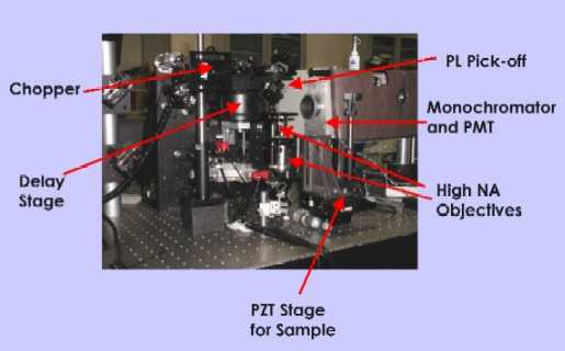
We have chosen to use multiphoton microscopy [1] as a possible alternative method. Multiphoton Microscopy is a derivative of confocal microscopy with improved resolution and depth sensitivity. Here, an ultrafast laser beam is focused on the sample with a high numerical aperture microscope objective. This excites photoluminescence (PL) in the sample through multiphoton absorption. The reflected part of this PL is caught by the same objective and collimated. A beam splitter picks off this PL and sends it to a monochromator to be detected. Since multiphoton excitation is a non-linear process (2nd order in the two-photon case), the PL is only excited in a small volume about the focus, where the light intensity is high. This gives the depth resolution. Also, since an ultrafast pulse is used, the average power is low, decreasing the chance of damage to the sample.
This technique will enable submicron resolution. However, in order to push the resolution limit to below 100 nm, 4-pi microscopy was developed [2]. Here, a second arm is added to the setup, a mirror image of the first. The ultrafast beam is split in to two and sent through these arms. When they meet at the sample, they will form an interference pattern at the focus if the pulses overlap in time and space. This effectively doubles the numerical aperture of the microscope. The 4-pi refers to a complete sphere in steradians. Using multiphoton excitation in such a setup increases the resolution by eliminating the side lobes of the excited interference pattern.
Below is the current version of our setup:
References:
- "Two-photon Laser Scanning Fluorescence Microscopy", W. Denk, J.H. Strickler and W.W. Webb, Science 248, 73-76 (1990).
- "Properties of a 4Pi Confocal Fluorescence Microscope", S. Hell and E.H.K. Stelzer, JOSA A 9, 2159-2166 (1992).